
Three things compound semiconductor’s fate
This article is from the CW Journal archive.
The four most dangerous words in the semiconductor industry lexicon might be: ‘It’s different this time.’
This phrase is often asserted when justifying the marking out of strategic positions or market prognostications.
Since the early days of semiconductors, compound devices have been the next big thing but, so far, they have never managed success beyond a few highly specialist niches. High device costs plus ever-improving silicon performance have constantly moved the market goal posts, meaning they have never been able to gain market traction or achieve the production volumes necessary to realise the cost benefits of scale. They have only found use in applications for which performance was more important than cost, for example military and space, or those few commercial applications for which no other viable silicon option existed, such as power amplifiers for smartphones and other wireless devices.
That is, until now, it seems. The recent trends in automotive and wireless (5G) have driven an increased fervour for compound semiconductor devices. This poses the obvious question… are things actually different now?
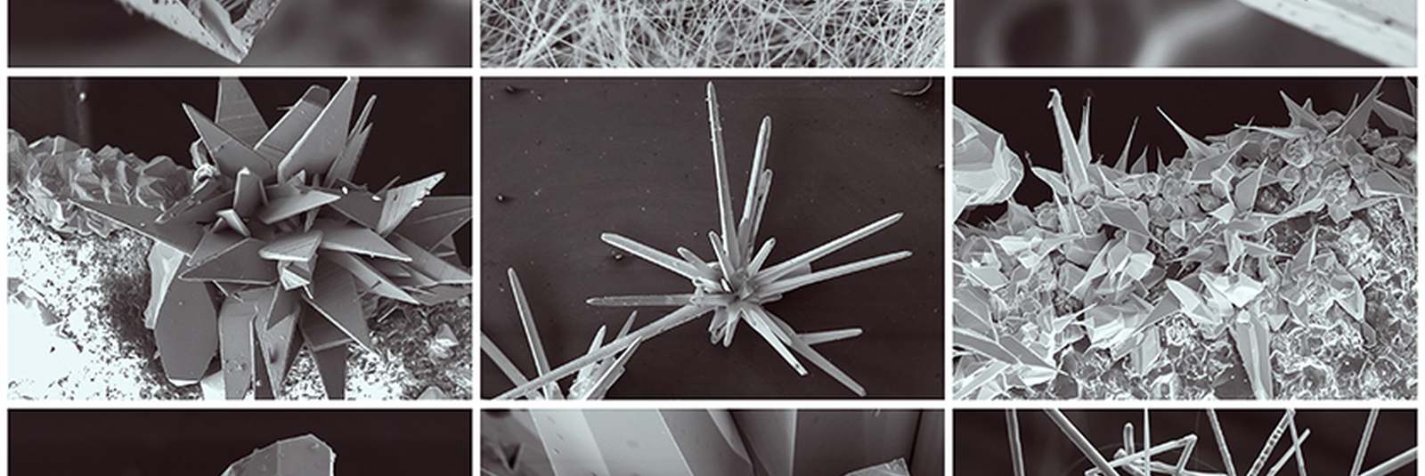
Compound semiconductors research began as far back as the mid-1950s, but development of parts for commercial use took a long time. There were a number of reasons for this: the difficulty of growing compound crystals, the high number of defects in the crystals, the fragility of the crystals and the high cost of production relative to silicon.
As with all new technologies in the chip industry, two hurdles were almost impossible to jump over. First, there was an industry-wide resistance to a move from the incumbent silicon technology; firms preferred instead to squeeze every last breath of life (and performance) from the tried and tested process. This was driven both by the cumulative manufacturing experience and high sunk investment cost. The ‘if it ain’t broke, don’t fix it’ mantra was, and still is, a huge industry barrier, and it’s been incredible to see how successful silicon development has been.
Second, the high cost of making the compound wafer substrates and the low manufacturing yields priced devices out of reach for most commercial applications. While the cost of making compound semiconductors has come down, it is still far higher than that of the production of silicon semiconductors.
Offsetting this disadvantage, the technology’s better performance has never been in question, and the properties of the crystals mean they can be used to do things that are not possible with silicon, justifying the cost where performance needs prevail. But too often price has been an overriding factor. The industry tends to favour being cheap and good enough rather than offering the best performance.
So manufacturing cost has been the compound semiconductors’ Achilles heel.
Compound semiconductors’ performance advantage stems from the fact that electrons in compound semiconductors move much faster than those in silicon. The materials also operate at much lower voltages, can emit and detect light, withstand higher levels of radiation and work at much higher temperatures. This means they can function better than their silicon equivalents, and at much lower energy levels, improving performance for current applications and opening the way for new applications that were previously impossible with silicon-based solutions.
Three forces are currently in play which seem set to knock over the hurdles.
The first of these is on the manufacturing side, as the industry no longer relies on compound wafers; rather, it has mastered the technique of growing films on top of silicon substrates. Gallium nitride (GaN) on a silicon wafer is a lot cheaper to make and device yields are much better than when compound wafers had to be made from scratch. The process is also less of a radical departure from the industry status quo.
Second, market opportunities in automotive and next-generation wireless are providing a ‘right place, right time’ moment for the technology, with these new systems operating at frequencies not even dreamt of a few years ago.
The third factor is that silicon is running out of steam for many applications. In the past, to compensate for the fact that the silicon world was not perfect, companies simply pushed the substrate beyond its technical limit. These techniques have been hugely successful, be it in manufacturing work-arounds or clever control of the device physics, but the options have now either reached their practical limits or are no longer worth the effort.
It seems now that the compound semiconductor industry’s perseverance is starting to pay off, and compound semiconductors have started to gain sizeable market traction, for example gallium arsenide (GaAs) for radio frequencies (RF) and photonics, and silicon carbide (SiC) for RF and power.
All of them follow in the wake of the long-held market lead for GaN for light-emitting diodes (LEDs).
Today’s systems and photonics are creating the market pull for compound semiconductor substrates. With a closing cost differential and growing natural market demand, these forces might now constitute a perfect opportunity for these materials.
Whilst still very small in absolute value terms – just US$120 million in 2019, compared with the US$400 billion total semiconductor market – the compound semiconductor market could easily reach four times this size by 2024, which would represent a compound annual growth rate of around 27 per cent. This compares with an eight per cent overall semiconductor market growth over the same period. This high growth rate is typical of any new industry sector at the start of its cycle; what makes this stand out and seem unrealistic is that such a growth rate has been such a long time coming.
|
DO YOU HAVE A VIEW ON THIS SUBJECT, OR RESPONSE YOU'D LIKE TO SHARE? |
Analog Devices (US),
Broadcom (US),
Cree (US),
Efficient Power Conversion (US),
GaN (Canada),
Infineon (Germany),
IQE (UK),
Lumentum (US),
Mitsubishi Electric (Japan),
NeoPhotonics (US),
Nichia (Japan),
NXP Semiconductors (The Netherlands),
ON Semiconductor (US),
OSRAM (Germany),
Qorvo (US),
Rockley Photonics (UK),
Samsung Electronics (South Korea),
San’an Optoelectronics (China),
Skyworks (US),
STMicroelectronics (Switzerland).

Power electronics has been one of the early emerging markets, driven by renewable energy and electric motor drives and the dual need for enhanced device performance and reduced power consumption. These opportunities have provided a huge boost to, in particular, silicon carbide power devices.
Photonics also provides a big market potential across a wide range of applications and materials, given that the wavelength required is determined by the bandgap of the material. Different materials are needed throughout the shorter to longer wavelengths in the spectrum.
One of the biggest issues has been the opinion that compound semiconductors are a replacement for silicon, just as silicon replaced germanium, PMOS replaced bipolar, NMOS replaced PMOS and CMOS replaced NMOS. In some instances, this may be true, for example in power devices, but in the majority of cases compound semiconductors will co-exist with, and complement, silicon, which will continue to be the mainstream technology of choice. It is thus better to consider the true role of the compound semiconductor industry as more symbiotic than supplantery, helping to grow the overall semiconductor market by enabling new applications to be built that were previously impossible in an all-silicon world. This expansionist role is a classic semiconductor story and, along with Moore’s Law and the industry cost learning curve, has been a key factor in driving the chip industry to its current US$400 billion size.
One such example of a new application not previously possible is in satellite communications, in which a low-cost compound semiconductor solution can fulfil both the high-frequency RF needs and reduce the power and weight requirements. The combination of better device performance and the fact that these materials can operate in a high-radiation environment without the need for screening, whereas silicon is susceptible to soft errors and has to be screened, has opened the door to production of small, light and cheap satellites that cannot be made
using silicon.
In the automotive arena, the market potential spans increased types of driver- assistance tools (and eventually, the much over-hyped autonomous vehicles) on the one hand, and the migration towards electric vehicles and the associated power electronics challenge on the other. The automotive sector has been a major driver of the semiconductor industry for several years, with the electronics content in a car now the single biggest cost of mamanufacture. The new system opportunities made possible by compound semiconductors will expand and help underpin the continuation of these high growth rates for the foreseeable future.
On the manufacturing technology front, bulk GaN wafers have been around for some time in, for example, laser diode applications. These have now started to appear as a competing technology to SiC in power electronics as well as in emerging RF applications. The winner will ultimately be determined by which solution offers the best overall technology-cost benefit.
Early compound semiconductor devices relied on bulk crystal material, which made them prohibitively expensive. Today the industry is driven by engineered substrates, and even though the substrates remain expensive compared with silicon, the market is now showing signs of finally taking off.
Silicon has been the chip industry’s workhorse for the last 60 years, and will continue to be so, but its physical limits are now being reached. It suffers from relatively poor electron mobility, restrictive transistor switching speed and a need for higher operating voltages compared with compound semiconductor devices. It does not perform well at high temperatures and is not very good at dealing with light.
This latter issue is starting to have a real impact on demand as the need for photonics in system design increases.
GaN is one of the most prominent compound semiconductor materials. Its major application is in lighting, power and RF devices. GaN devices will also play a major role in 5G wireless. In the military segment, GaN applications vary from electronic warfare to radar to communications. GaN-based power devices also play a key role in the power conversion market, in which they offer similar performance benefits to those offered by SiC parts, but at lower cost, because GaN power devices can be grown on larger, cheaper silicon substrates than SiC can.
Telecommunications is expected to become the largest market share of the compound semiconductor market, owing to increased usage of compound semiconductors such as GaAs, GaN, InP and SiGe in 5G roll-out. GaAs is the current technology of choice for powerful and low- noise amplifiers, due to its superior linearity performance.
Industries can be predicted to progress through four distinct stages: Stage 1 (Opening), Stage 2 (Scale), Stage 3 (Focus) and finally Stage 4 (Balance and Alliance).
Stage 1 generally begins with a single start-up or the emergence of a technology, and quickly fragments as companies jump on the bandwagon. That happened in the 1950s for compound semiconductors.
In Stage 2, players focus on building scale and establishing market position. They focus on building market share and squeezing out competition, with some failures and early consolidation. For compound semiconductors, this erratic stop-start, stall and reset process has yet to run its course.
With leadership positions established, Stage 3 heralds a major drive on focus with the clear aim to be the ‘last man standing’, leading to an inevitable saturation in market share. This is without doubt the most challenging stage, with many losses and casualties, either through acquisition or failure.
Stage 4 then turns to development and maintenance of competitive positions through mergers and acquisitions.
Currently, the fragmented and immature market is typical of Stage 2, with firms and technologies vying for supremacy.
As the industry moves towards Stage 3, several of the vendors will have left the market through mergers and business failures.
The good news is that demand is now increasing and winners will emerge. These may not always offer the best technological solution: in fact, companies would do well to remember that, in the chip industry, first and good enough today wins compared with offering a better solution tomorrow.
The real test will be whether the price is right.
That poses more of a business than technical challenge. This is not just a manufacturing problem but a battle for corporate survival. Once any industry becomes interesting enough to be noticed, it no longer becomes a comfortable minority niche but an invading force in waiting.
The biggest industry challenge will not be the physics or the technology, but which company will be successful in establishing market share. This is not a fight for the financially weak or faint-hearted.
The market is likely to end up dominated by three major firms with a combined 90 per cent market share. Consolidation is inevitable and casualties unavoidable.
|
GET CW JOURNAL ARTICLES STRAIGHT TO YOUR INBOX Subscribe now |
Malcolm Penn is a leading global semi-conductor industry analyst with over 50 years’ experience covering all aspects of the semiconductor and electronics industry supply chain. Prior to establishing his Future Horizons consultancy,he held roles in operations, marketing and business development in the semiconductor and electronics industry, having worked his way through university as a professional musician.