Speakers

Charles Sturman

Haydn Povey

John Boston

Speaker Session
As the semiconductor industry looks to move beyond the current AI wave, this session assesses the UK’s current position in the globally competitive semiconductor ecosystem: our strengths, our gaps, and the opportunities that lie ahead. With a focus on what comes next - from photonics and power electronics to heterogenous integration - we will explore how the UK can shape and lead in the next frontier of technology.
|
Tony Pearce, COO, Paragraf |
|
Haydn Povey, CEO, SCI Semiconductors |
|
John Boston, Managing Director, Custom Interconnect Ltd |

As the CEO at TechWorks, Charles drives collaboration between industry, academia and government, promoting the Deep Tech sector and helping grow new technology business across the UK.
Charles is also a mentor and advisor with several accelerators and incubators. Previously, he held executive roles in GM, product line, go-to-market, business development, corporate strategy, and new business venturing at HiSilicon, u-blox, ARM, Acorn Computers and Motorola and has been instrumental in two successful start-ups.
With 30 years of experience in VLSI chip design, embedded systems, IoT, computing and wireless communications (2G, 3G, LTE, Wi-Fi, and Bluetooth) Charles is the author of numerous papers and books and holds a master’s degree in electronics & information engineering from Southampton University.
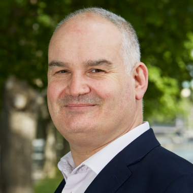
Haydn Povey is CEO of SCI Semiconductors, and a veteran of the embedded design space. Starting his career at National Instruments, he was hired into Arm to lead the deeply embedded processors, leading the Cortex-M family and working across global silicon vendors to drive adoption of the new technology. At Arm he also owned the security technology portfolio, including TrustZone, that underpin security across mobile phone, automotive and industrial applications. Following Arm, he founded Secure Thingz, a successful security startup, which was purchased by IAR Ltd, the leading tools vendor, where he was Group Chief Strategy Officer for over 5 years.

John has over 47 years’ experience working in semiconductor packaging and electronics assembly technology, all of which has been in industry. Starting in STC Paignton in 1978 in their Thick Film Hybrid division and then transferring to their high reliability Optoelectronic Division. Over the next 11 years, he worked everything from Laser and LED die bond / wirebond, fiber-optic alignment, hermetic lid sealing, leak checking, life testing and failure analysis for Hi-Rel optical communication systems that would ultimately see STC being acquired by Nortel Networks. He joined Custom Interconnect Ltd (CIL) in 1989, where he remains after 37 years. The first 6 years were spent as a Design Engineer / Design Manager / Technical Manager on semiconductor packaging / complex PCBA’s and in 1995 he became Operations Director of CIL and Managing Director in 2001. In 2023, CIL opened its BP2 facility which is the UK’s largest OSAT facility and CIL is the UK’s 3rd largest EMS provider with a turnover of £45M this year and planned turnover next year of £75M.
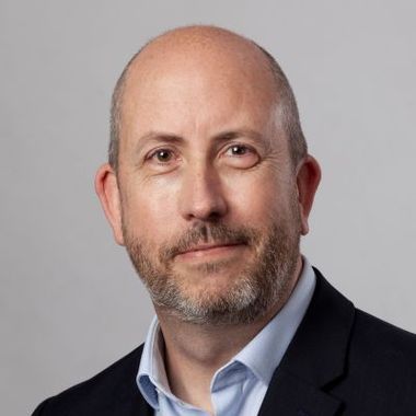
With over 30 years’ experience in the semiconductor industry, Tony Pearce is COO at Paragraf, responsible for scaling the business from start-up to high volume manufacturer. His background includes previous positions as Managing Director with semiconductor equipment manufacturer Aixtron Ltd, and as VP of Global Operations for compound semiconductor manufacturer IQE plc. Specialising in establishing and growing manufacturing facilities, capabilities and organisations commercialising breakthrough technologies spanning from advanced semiconductor equipment to graphene electronics.