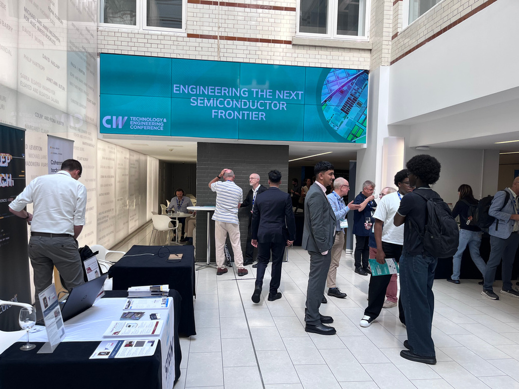
CWTEC: Engineering the next semiconductor frontier
Attendees were rewarded for battling through heat and delayed trains by a fantastic array of speakers from organisations doing exciting things across the UK, exploring the topics of capability, connection and indispensability.
Throughout the day, a number of key themes and discussion points emerged:
AI is changing the game - at both a need and a development level
No conference is complete these days without reference to the impact of AI and CWTEC was no exception. Multiple speakers across the day referenced the unparalleled demand for compute, which in turn is driving up semiconductor demand and pace. Prof. Tony Kenyon from Neuroware commented that compute requirements are doubling every 2.5 months yet “our capability to provide that is not scaling at anywhere near the same rate”.
This huge demand is being driven largely by AI where we’re seeing up to 35 quadrillion tokens being generated per month - 12-13x growth year on year. A large part of this is the growing capability of the AI models themselves; we’re seeing smarter models, longer tasks and a consequent explosion in the tokens we need to generate. Inference speed is now the bottleneck.
Different organisations are taking different approaches to addressing this. UK based company Fractile is focused on the high bandwidth memory (HBM) wall, where compute is outstripping memory and sits waiting for data to be served to it. Long contexts in AI models are just compounding the problem. They’re addressing this memory wall through their own integrated memory and logic, achieving much higher bandwidths but with economics comparable to HBM models.
Others are looking at new materials to create a paradigm shift and address the fact that silicon doesn’t offer solutions to the factors holding AI back: the speed, the complex GPUs waiting for data, and energy consumption. Dr. Rodney Peizel, CTO and COO, IQE plc, made the case that compound semiconductors can address these points directly from the edge to the chip: “the entire end-to-end chain has compound semiconductors in every single step and that’s why we’re migrating to new materials, because compound semiconductors do what silicon begins to fail to do.” He spoke to gallium nitride as one particular example that can facilitate huge power reduction, enabling up to 5% more compute capacity with the same power budget.
Prof. Jon Hefferman, Director, National Epitaxy Facility, University of Sheffield, also spoke to the need for new materials to meet specific requirements from advanced applications like AI, but also neuromorphic, quantum, space compatible electronics and more.
He spoke compellingly about how AI is not only driving this need but can also play a significant role in finding new materials. Hefferman argued that the semiconductor sector should be taking its lead from the pharmaceutical industry where AI has been used successfully for drug discovery and notably reducing time to develop. When it historically takes 20-30 years for a material to transition from lab to global industrial scale (commercialised to a $1bn market), any time saved could have a significant impact.
He noted that Google and Microsoft are already conducting AI-assisted inorganic materials discovery which has been very successful for batteries and opens up opportunities for semiconductors.
“AI is currently our telescope, scanning the known space” he said. “But the revolution will be AI shifting paradigms of functional design.”
The UK is demonstrating true innovation
There was much talk throughout the day of the UK’s great heritage when it comes to semiconductors and that this pedigree gives us a significant platform to jump from. Charles Sturman, CEO, TechWorks, provided some stats to back up the claims, with UK semiconductors contributing £11bn in revenue and representing 2% of global revenue share. As he remarked, “it may not be as large an industry as it was in the UK, or as large as other leading economies, but we have a good baseline to start building from and there is a strong government focus, recognising the foundational element of semiconductors for all other elements of the industrial strategy.”
Janet Collyer MBE, Portfolio NED, echoed this sentiment, identifying two key building blocks for the UK: technology and talent. Both of which became clear in abundance throughout the day as we heard from numerous UK-based organisations doing innovative and exciting work in the field:
Paragraf - have created the world’s first 2D material foundry with a unique method of graphene wafer production that is directly grown on electronic grade substrate. The UK now has the only device fab dedicated to 2D materials and is leading research globally.
Finchetto - identified that there is no universal material that serves all needs and has been working with TFLN (Thin Film Lithium Niobate) as a solution that offers a combination of materials that is extremely difficult to match for photonics. Using TFLN, they have developed all optical ethernet switches offering no buffering, 300ns port-to-port latency (7x faster) and 48W total power consumption (98% lower than state of the art). This market is commercially significant and likely to be low volume, high value manufacturing - exactly the sort of opportunity the UK could succeed at.
Quantum Dice - have developed a full processing platform designed for massive probabilistic processing. Doing it faster and with less energy than traditional compute. Probabilistic computing needs probabilistic hardware and algorithms but they haven’t scaled because of the sampling bottleneck - at scale, the sampling overwhelms conventional processors. Up to 70% of compute can be spent on sampling rather than undertaking the end task it’s supposed to be doing. Their PPU (probabilistic processing unit) removes the bottleneck by enabling 1000x faster sampling, powering probabilistic computing at scale, for the first time.
Lumai - have taken a ground-up approach to using optical compute for AI that is scalable, looking at materials that are very mature and already driving data centre compute. They have developed a hybrid architecture where optical handles the compute bottleneck, while digital delivers on everything else. Unlike silicon - where efficiency decreases with performance - Lumai’s optical solution delivers efficiency that increases with performance. They’re on track to deliver 95% reduction in energy (enabling maximisation of compute for the same energy budget) and 90% reduction in total cost of compute (reducing capital costs for compute) by 2029.
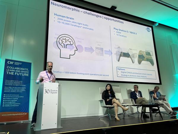
Neuroware - the UK Innovation and Knowledge Centre in Neuromorphic Computing Hardware is exploring the opportunities available to the UK from neuromorphic computing. The brain has a high degree of power efficiency but it also deals well with imprecise, uncertain and noisy data: there is plenty of inspiration to take from the brain. The UK is well placed to explore neuromorphic as a novel type of compute, sitting alongside digital and quantum.
Throughout the day it became clear that it’s not just our heritage in the UK that we should be proud of, with a huge diversity of organisations, focuses and skills leading the way in engineering the next semiconductor frontier.
The focus on sovereign capability creates an opportunity - but we have to approach it in the right way
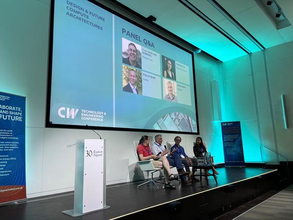
“Semiconductors are the oil of our generation,” said Dr. Rodney Pelzel and indeed there is no getting away from the fact that alongside regional specialisation throughout the semiconductor value chain, geopolitics is rewriting the rules of the game as we encounter warfare, trade barriers and races for critical materials. A repeated message throughout the day is that there is significant opportunity here for the UK but that we have to be realistic because we can’t make everything here (and even if we tried we would still need to source materials). As Alex van Someren, Executive Chair, Photonic Inc, succinctly put it, “we’re never going to be Taiwan” but we do have “lots of strengths and skills in the UK and we want to make sure we can get the most out of them”.
Our opportunity therefore lies in being strategic about selecting the critical parts of the supply chain we can make and where we can build specific areas of excellence and expertise. Or as Steve Taylor, Director of Strategic Marketing, UK Semiconductor Centre, put it, “what can we do and what can we scale?”. He introduced the concept of indispensability, which was raised many times throughout the conference, stating the need to create something that others see we do, realise they need and are willing to spend money on.
An interesting topic of discussion was raised by Prof Gary Graham, Professor in Operations Management, Liverpool John Moores University, who introduced the concept of strategic bottlenecks in the semiconductor industry.
Chokepoints or bottlenecks can be seen as dynamic sites of leverage that can be created, mitigated or dissolved through policy, ownership or regulation. And in a world where the UK needs to pick its battles and work out where it can take a leadership position, consideration should be given not just to what we’re good at but the power we hold and the role of strategic understanding and negotiation. “If you own part of the supply chain”, said Pelzel, “you have leverage to negotiate access to other parts”. This was echoed by Janet Collyer who stated that it’s possible to be strategically significant without being the biggest player.
And we can’t just look inwards. Prof Andy Sellars, Director of Strategy, Cornerstone, observed that while there is lots of momentum happening in the UK government we also need to be conscious of what other countries around the globe are doing. “There’s no point going head to head with something already in existence,” he said. “Playing catch up is time consuming and expensive”. He went on to observe that there are no dominant players in the edge AI market for instance, the photonics quantum platform is built on mature tech and is therefore scalable, and neuromorphic offers considerable potential.
One other opportunity - which would offer practical as well as strategic value - is the creation of a pilot line to support these developing technologies. Offering modest volumes and consistent processes, this would feed into the larger ecosystem enabling system integration companies to scale up. Sellars believes this pilot line would be the first in the world giving us a significant first mover advantage.
The speakers were aligned on the fact that we need to be indispensable in specific areas of strength while avoiding dilution of competing everywhere. We can’t just lift what’s being done in another country, we have to innovate and there was plenty of evidence throughout the day that’s exactly what is happening. The UK is well known for having expertise in design and IP but there was a strong sense that there are more areas where we can shine and we should be ambitious in exploring opportunities such as high value, low volume.
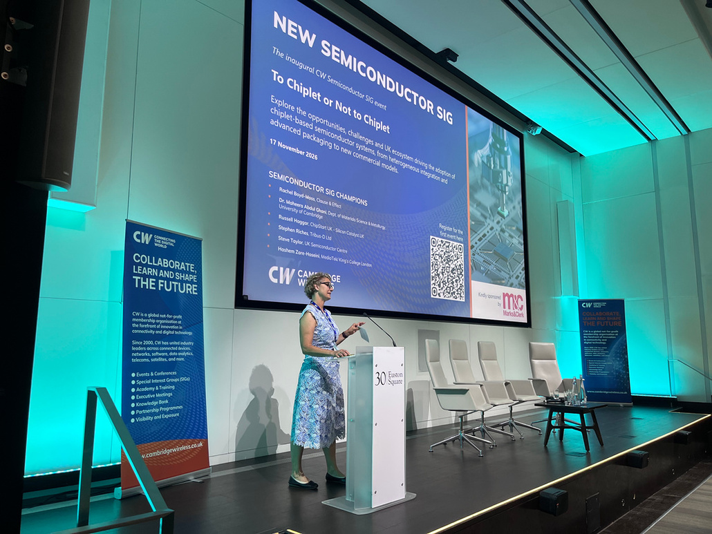
The day also saw Cambridge Wireless announce the formation of a new Semiconductors Special Interest Group, sponosored by Marks & Clerk, with their inaugural event - To Chiplet or Not to Chiplet taking place on 17th November. Full details available here.