Integrated GaN solution revolutionises power supply design
World’s first integrated GaN and gate driver
The new MasterGaN® product family from STMicroelectronics is the world’s first platform of integrated devices embedding a gate driver based on silicon technology along with a pair of GaN transistors into a single device. The combination brings a quantum leap in power performance by providing robust, efficient, and high-power density whilst at the same time simplifying the design of power systems. They will are accelerating the creation of next-generation compact and efficient chargers and power adapters for consumer and industrial applications.
Today’s GaN market is typically served by discrete power transistors and gate driver ICs that require designers to learn how to make them work together for optimum performance. STMicroelectronics MasterGaN approach bypasses that challenge, resulting in faster time to market and assured performance, together with a smaller footprint, simplified assembly, and increased reliability using fewer components. Utilising GaN technology and the advantages offered by STMicroelectronics integrated products,
As the first integrated GaN and gate driver solution to the market, MasterGaN is allowing the realisation of these more compact, lighter, and highly reliable chargers and power supplies which require less design effort.
The Integration of the GaN transistors and gate drivers into a single device provides many benefits, it offers high efficiency due to an optimized gate drive layout, high power density and increased switching frequency due to minimal parasitic effects, in addition it helps to simplify the design with a compact single-chip solution.
Common Topologies
Firstly, let look at some common power topologies to see how GaN based devices can offer benefits.
A great example demonstrating the benefits of GaN devices can be seen with a typical flyback converter design. A common solution is where the flyback converter very often has a passive snubber to reduce the peak voltage on the primary FET, induced by the leakage inductance of the transformer, this is to allow the circuit to meet EMC standards.
This power dissipated in the passive snubber is essentially wasted energy, it can be calculated using the measurements of key criteria of the snubber design including, VCLAMP which is the voltage across the snubber when the primary FET is OFF, the transformer turns ratio and the transformer peak primary current.
By using GaN devices and employing an active clamp topology, instead of wasting the leakage inductance energy, the active clamp circuit can be used to improve efficiency by storing this previously wasted energy in a capacitor, then delivering it to the output later in the switching cycle.
Typical application diagram – Active clamp flyback
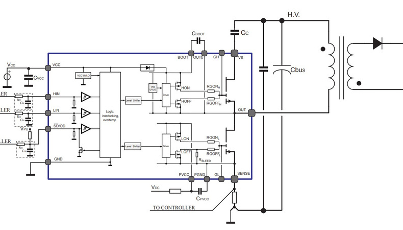
The area contained within the blue box represents the MasterGaN device.
Furthermore, combining TM (Quasi resonant) operation with an active clamp can completely remove the switching loss, allowing the switching frequency of an active clamp flyback to be higher, thus reducing the overall size of the power supply.
Another common topology, totem-pole power factor correction (PFC), is widely used in applications where high efficiency is required. A conventional PFC design consists of a Bridge rectifier followed by a boost converter consisting of three main components: inductor, power MOSFET and a diode rectifier, usually a SiC diode if using continuous current mode (CCM) boost.
In a totem-pole PFC these parts can be replaced by two GaN transistors, two SiC diodes and one inductor. Its main benefit compared to the conventional boost PFC is that it is a bridgeless circuit, meaning that it does not include a rectifier diode bridge at its input. Therefore, the associated rectifier bridge losses are eliminated, leading to higher efficiency and power density.
MasterGaN Family
The MasterGaN family of devices span different GaN-transistors and are offered as pin-compatible half-bridge products that let engineers scale successful designs with minimal hardware changes. Leveraging the low turn-on losses and absence of body-diode recovery that characterize GaN transistors, the products offer superior efficiency and overall performance enhancement in high-end, high-efficiency topologies such as flyback or forward with active clamp, resonant, bridgeless totem pole PFC (power factor corrector) and other soft- and hard-switching topologies used in AC/DC and DC/DC converters and DC/AC inverters.
The MasterGaN family is currently available in mass production across three devices with more on the future roadmap. The first device is MasterGaN1 which has been optimised for Resonant LLC and Active Clamp Flyback converter topologies up to 400W. The MasterGaN2 device is suited to soft-switching and Active Clamp Flyback converter topologies up to 65W whilst the MasterGaN4 device is suitable for Resonant LLC and Active Clamp Flyback converter topologies up to 200W.
The MasterGaN family of advanced power system-in-package devices all integrate a gate driver and two enhancement mode GaN transistors in a compact package. MasterGaN1 and MasterGaN4 devices are configured in a half‑bridge and MasterGaN2 employs an asymmetrical half bridge configuration.
The integrated power GaNs have an RDS(ON) of 150 mΩ for MasterGaN1 and RDS(ON) of 225 mΩ for MasterGaN4 devices for both Low side and High side. For the asymmetrical MasterGaN2 devices the integrated power GaNs have an RDS(ON) of 150 mΩ and 225 mΩ for Low side and High side, respectively. The MasterGaN devices all have 650 V drain‑source breakdown voltage, while the high side of the embedded gate driver can be easily supplied by the integrated bootstrap diode.
The MasterGaN1 device is capable of maximum continuous drain current IDS(MAX) of 10A and the MasterGaN4 device has an IDS(MAX) of 6.5A for both the High side and Low side. The asymmetrical MasterGaN2 device offers an IDS(MAX) of 6.5A and 10A for the High Side and Low Side, respectively.
The MasterGaN devices all feature UVLO protection on both the lower and upper driving sections, preventing the power switches from operating in low efficiency or dangerous conditions, and the interlocking function avoids cross-conduction conditions. The input pins extended range allow for easy interfacing with microcontrollers, DSP units or Hall effect sensors.
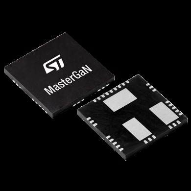
The devices are designed to operate over the industrial temperature range, -40°C to 125°C and are supplied in a compact 9x9 mm QFN package.
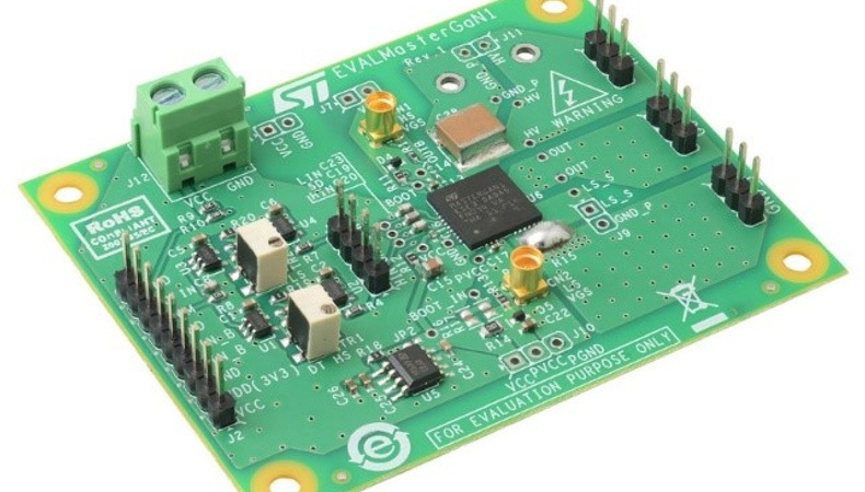
To assist designers, STMicroelectronics have also made available development boards which are easy to use and quick to adapt tools to evaluate the characteristics of the MasterGaN family of devices. The boards help designers quickly create new topologies without the need of complete PCB design. The boards provide on-board programmable inputs deadtime generator with a single VCC supply and an embedded linear voltage regulator offering 3.3 V rail to supply low voltage logic circuits like microcontrollers or FPGAs.
The boards all incorporate spare footprints allowing designers to customise the boards so they can be integrated into the customers final application. The boards can be further customised to allow the use of a separate input signal or single PWM signal, use of external bootstrap diode, separate supply for VCC, PVCC or Vbo and also the use of low side shunt resistor for peak current mode topologies. The boards give access to all pins of the MasterGaN devices further extending flexibility. The development boards measure just 56 x 70 mm wide and use a standard FR-4 PCB delivering an impressive thermal resistance Rth(J-A) of 35 °C/W, without forced airflow.
Conclusion
To summarize, by integrating GaN devices and gate drivers into the same device package the MasterGaN family offers a wide range of benefits over traditional silicon-based solutions including:
Higher efficiency – Reduced power losses, reduced power consumption, which exceed the most stringent energy requirements.
Higher power density – Higher switching speeds also enable reduced system size and cost.
Faster go-to-market – Packaged integrated solution simplifies the design and at the same time gives a higher level of performance.
Anglia offer support for customer designs with free evaluation kits, demonstration boards and samples of STMicroelectronics products via the EZYsample service which is available to all registered Anglia Live account customers.
Anglia’s engineering team are also on hand to support designers with their extensive experience of working with power system designs and can offer advice and support at component and system level. This expertise is available to assist customers with all aspects of their product design, providing hands on support and access to additional comprehensive STMicroelectronics resources including technical application notes and reference designs.
Visit www.anglia-live.com to see the full range of STMicroelectronics products available from Anglia.